| |
Digital Storage Oscilloscope Adapter |
|
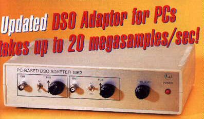
es, it's finally here !. The DSOA Mk3 has been a long time coming (many years in fact), but it was finally published in the October/November 98 issues of EA.
EA October 98 issue cover shot of DSOA Mk3
Here are the basic specs :
* 20MS/s
* 5MHz analog bandwidth (*see below)
* Dual channels
* Optional external trigger input.
* PC-Based, connects to standard parallel port.
* Easy to build on one single sided pcb.
* Vertical position adjustments.
* Fully software controlled timebase and attenuation rages.
* 100ns/div to 50ms/div timebase in 1-2-5 sequence.
* 100mV/div to 5V/div vertical ranges in 1-2-5 sequence.
Well, it looks like I was way off the mark with the design of this Mk3. Hundreds of previous users said they would love something like this, and would pay anything to get it. Well, while this may be true, it looks like no one wants to even think about building it if there isn't a full kit available. A few people have expressed interest in a short form kit, but overall the entire project is a flop :(
The major kit suppliers in their infinite wisdom have decided not to kit up for the project, apparently because it is too expensive. There has been an expression of interest from other people about doing a short form kit, but this may or may not eventuate. No matter how good this design is, it is a complete flop simply because there is no kit available.
Current Status :
This is my current stance on this project, please do not email me (or call me) and ask what the current status is, because this is the current status. If anything changes, I will change this :
I am NOT selling a kit (either full or short form), the PCB, or any components, and have no plans on doing so.
I do NOT know anyone, anywhere in the world, who is selling any sort of kit.
As far as I know, the PCB is available from RCS radio, for something like A$58.
ALL of the parts are available from either RS Components, Farnell Components, Jaycar Electronics, Altronics, Dick Smith etc. RS and Farnell stock the "hard to get" chips. I live in Australia, and these are all Australian companies, I have no idea where you can get the components in other countries. UPDATE - I have heard that the TDA8703 ADC chip is being discontinued, please check this before proceeding with this project.
I have no plans to finish the Windows software to a point where I would be happy to sell it commercially. Sorry about that, but because of the lack of interest, it is not worth my while.
I am *NOT* providing comprehensive support for this project (or any project for that matter). I will answer general questions, but I do not have the time to support every aspect of it's construction with you. Basically, you build it at your own risk, the same as every other published magazine project, I don't know why people think this one is any different. This is an advanced project and if you do not have the technical skills to troubleshoot the project if it does not work then you shouldn't even attempt it.
What is the Bandwidth ?
There seems to be a lot of confusion about the bandwidth of a real time digital cro such as this project and the previous Mk1 and Mk2 designs. A lot of people keep asking what the bandwidth is, and seem to forget (or don't know) the basics of digital cro's. There is a big difference between sample rate, analog bandwidth, and effective bandwidth. I will clarify this situation now :
Sample Rate :
A real-time digital cro samples in real-time, ie, it takes one sample after the other. In the case of the Mk3 this is 20MHz. This 20MHz is NOT the bandwidth of the cro, it is the real-time sample rate of the analog to digital convertor.
Analog Bandwidth :
The analog bandwith is the -3dB bandwidth of the analog input amplifers and associated circuitry BEFORE the ADC. In the case of the Mk3 design, it is roughly 5MHz.
Effective Bandwidth :
The effective bandwith is a rule of thumb, which is basically 10 times less than the sample rate, or 2MHz in this case. This comes about because you need at least 10 samples per cycle of the signal you are measuring to get any decent waveform to actually view.
Now, to answer everyone's question, the effective bandwidth of this Mk3 design is roughly 2MHz, which gives you 10 samples per cycle. The analog bandwidth may be 5MHz or more, but if you try and measure a 5MHz signal you will only get 4 samples of your waveform which is next to useless. If you measure a sine wave you will see something like a triangle wave!.
If you want a real-time 20MHz bandwidth digital cro, then you need a sample rate of at least 200MHz, which quadruples the price and complexity, that's just the way it is.
For example, the new Tektronix TDS200 series real-time CRO's have a 100MHz effective bandwidth by virtue of a 1GHz sample rate. All the manufacturers are heading this way, as the interleaved sampling method (which allows high analog bandwidth with a small sample rate) is a dodgy way to do it, and manufacturers are finally learning this.
Back in February 1993, I described a design for a low cost PC based Digital
Storage Oscilloscope. Although relatively simple, the design was very popular
to say the least, with many hundreds of kits being sold.
A follow up Mk2 version described by EA's Jim Rowe in the May/June/July 94
issues of EA improved on the original with calibrated time and vertical
scales, and extra triggering features. This design proved even more popular
than the first, proving that there is a genuine need for such a low audio
bandwidth PC based scope.
It's probably no surprise then, to find that many people have asked for a
higher performance design, one with a bandwidth of several megahertz. Such a
device would have a much wider appeal, and be useful in a much greater number
of applications.
Ever since the original design was published I've received a constant stream
of requests for an updated design, along with many suggestions of what
features they would like to see.
Both previous kits have now been discontinued by most of the major kit
suppliers, and I felt it was time for an updated design. The result is the
design to be presented here. I hope it appeals to as any users as possible.
I wasn't able to incorporate all of features asked for in this new design, as
this simply wasn't possible. Some people wanted a portable battery powered
version, others wanted 4 to 8 channels, 100MS/s, 50MHz bandwidth, etc, etc.
By far the most number of requests were for three major improvements - higher
sample rate, dual channels, and more analog CRO like operation. The majority
of uses were simply using the DSOA as a normal analog CRO, with the added
benefit of single shot aquisition and waveform storage/printing of course.
Surprisingly, cost and ease of construction did not rate high on most user's
wish lists. However, I do consider these points very important, and
considered them carefully when designing this new DSOA.
The design to be presented here differs dramatically from the two existing
designs. It has four major new features - dual channels, 20 MS/s sample rate
(20 times that of the Mk2), fully PC controlled timebase and vertical
attenuation ranges, and vertical waveform position controls. At the same
time, this new design is not that much more expensive than the Mk2 design,
and is easier to construct.
The new design is still 8-bit resolution per channel, as anything more is not
warranted in a DSO (and would probably double the price !). Very few
commercial DSO's bother going beyond eight bits, and if they do it's usually
through software averaging.
There are 18 timebase ranges available from 100ns/div to 50ms/div in a 1-2-5
sequence, as well as 6 attenuation ranges from 100mV/div to 5V/div in 1-2-5
sequence. Both are fully adjustable by the PC software. The analog bandwidth
is at least 5MHz, but can be improved as will be discussed later.
Support for long term data logging has been dropped as standard, although it
is possible to use it for data logging given the right software. The
reasoning behind this being that 8-bit sampling and dual channels are not
sufficient for the majority of data logging applications. This is best left
to a dedicated design.
I have been often asked why I didn't do a version of the DSOA that uses a
plug-in PC card, either for the entire DSOA, or just for the interface. The
main reason apart from the extra cost and complexity, is that it cannot be
used with a laptop computer. At least with the parallel port the DSOA can be
used with almost any IBM compatible computer. Nearly half of all of the uses
of the previous Mk1 and Mk2 have used it with a laptop computer. I even know
of one user who has used a battery powered DSOA with a palmtop computer !.
People have also asked about utilising the enhanced parallel port standard,
which allows faster transfer rate. Once again it comes down to being
compatible with the most number of machines. Not every machine has an
enhanced parallel port, but they all have a standard parallel port.
Given all the new features in this design, it was not possible to use the
existing DSOA Mk2 interface and architecture, which makes the DSOA Mk3
incompatible with any existing software.
There are however two new software programs available. A simple DOS based
program that is provided free, and a complete Windows based program with dual
timebases, measuring cursors, averaging, history display, Windows printing
capability and more. Both of these will be discussed later.
DESIGN CONSIDERATIONS :
The first decision to make was that of the analog to digital converter, as
this single component would decide the upper performance limit of the design.
This was quite an easy task, as the only suitable easy to use high speed A-D
converter that is readily available in Australia at low cost is the Philips
TDA8703. This device can operate at a maximum sample rate of 40MS/s, so I
aimed for that sample rate as a maximum.
The next decision was the type of RAM's to use. This appeared simple at first
glance, standard cache SRAM's that are used on PC motherboards are very fast
(15ns), cheap, and readily available. I had even used them previously in my
PC-Based Logic Analyser Design. But after a bit of though, I realised there
was a catch.
Unlike the Mk2 version, I wanted the design to have 50% pre and post sampling
just like most commercial DSO's. This meant having two 15 bit counters, one
for the RAM address, and one for the post trigger counter. This requires 8
counter chips, quite a large number, and one that would require quite a deal
of PCB space.
I was tempted to use Programable Logic Devices (PLD's), but these are quite
specialised components that must be pre-programmed. I wanted to avoid this if
at all possible.
This is when I had the idea to use FIFO (First In First Out) RAM's. FIFO
RAM's are essentially SRAM's with inbuilt address counters, and also have the
capability to do 50% post counting as well !. This meant I could use one FIFO
chip to replace an SRAM and 8 counter chips, not to mention that the dual
data ports make the PCB layout a lot easier. They are also reasonably priced
and readily available.
However, FIFO's have three disadvantages. The first is that you can't use
only a part of the RAM, you must use it all (in this application anyway)
which means slower update rates. The second is that they are aren't quite as
fast as SRAM's, which would limit the maximum sample rate to 20MS/s. The
third being that they are only available in relatively small sizes (4-8KB at
most). Compared with the 32KB RAM size of the previous DSOA's, this may seem
some what limiting, but as I only wanted to design a CRO and not a data
logger, it isn't really a disadvantage. I decided that the advantages
outweighed the disadvantages (as I will show later), and I have thus chosen
them for this design.
The sample rate and buffer size in this design was therefore limited by the
FIFO's. But the good point is that they allowed me to fit the entire design
onto one single sided PCB. I originally started off with 4KB FIFO's, but
finally settled on 1KB devices as I will explain later.
I have opted to have both the attenuation and timebase settings fully
controlled from the PC. Although probably not as cheap (six relays are
expensive) or convenient as having controls on the front of the DSOA, it
drastically reduces the amount of internal wiring, and makes construction
easier. It is also easier to generate controls lines from the PC than it is
to read back front panel switch positions into the PC, which would have been
necessary had I used manual controls.
I have elected to have the trigger signal fixed on channel 1, and no facility
for an external trigger input as standard. The reasoning being that the
majority of users will seldom need both input channels AND an external
trigger input. Although it is relatively easy to fit an external trigger
input if required. This modification will be explained later.
HOW IT WORKS :
The heart of the DSOA is the TDA8703 ADC. This device is designed primarily
for video applications, and is very popular in commercial video equipment,
as well as other high performance PC based DSO designs as well. It is an 8-
bit "flash" type analog to digital converter with a maximum sample rate of
40MHz. The -3dB bandwidth of it's input buffer is the nyquist limit of
20MHz. It has selectable binary or two's complement 3-state outputs. The 3-
state output was not needed in this design due to the dedicated input port on
the FIFO RAM's. The DSOA uses the binary output mode by tieing the TC input
HIGH.
The TDA8703 requires only a single +5V supply, but it does have separate
analog and digital supply pins. It also has it's own internal reference
voltages of 3.26V and 1.55V, and thus requires a full scale input signal of
1.71V (3.26-1.55) biased by 2.4V. This requires the input signal to be
scaled and biased accordingly.
There are two input channels with identical analog circuitry, so we will only
discuss channel 1 here. The input from the probe comes in via a BNC
connector on the front panel. It either passes through C100 or is fed
straight through depending on the setting of the AC/DC coupling switch S4.
With S4 in the AC position, any DC voltage present in the input signal is
removed. The signal is then applied to the input voltage divider formed by
R28, R29, R30, which divides the signal by 10. The total resistance of the
voltage divider is 1Mohm, which allows the use of standard x10 CRO probes.
The divided by 10 signal is fed along with the original input signal into
range selection relay RLY4. This relay which is under software control
selects which amplitude signal will be fed through to the following buffer
stage.
With R28, R29, and R30 being such high values, any stray capacitance will
effect the division ratio when measuring any reasonably high frequency. Even
1pF of stray capacitance has an impeadance of 160K at 1MHz. This can
significantly effect the divider, and will show up on square waves as
overshoot or undershoot. To compensate for this, CV1 and C39 are used to keep
the division ratio constant at high frequencies.
The analog section was deliberately designed to avoid the use of multiple
compensation adjustments per channel, which are generally interactive, I.E,
adjusting one will upset the adjustment of the other. This design only has
one compensation adjustment per channel, and this avoids the often frustrating
task of adjusting multiple pots.
The selected signal is fed via R27 into the protection network formed by D5
and D6, which will clamp any input signal to +/-12.6V. The signal is then
buffered by IC20, a fast FET input amplifier wired in a non-inverting buffer
configuration. C37 is required to compensate the amplifier and prevent
overshoot on fast changing signals. The performance of the entire analog
section is dependant upon this first FET input buffer. C37 limits the
bandwidth and slew rate of the amplifier. With C37 equal to 5p6, the -3dB
bandwidth is approximately 7MHz, and the slew rate about 35V/microsecond.
This is adequate for a 20MS/s DSO, but higher performance may be achievable
by lowering the value of C37.
The buffered signal is then fed into the range compensation amplifier formed
by R31 to R37, IC21, and relays RLY5 and RLY6. This amplifier is wired in an
inverting configuration, and provides three different gains selectable under
software control by the two relays. The three ranges effectively provide the
1-2-5 voltage range sequence like a normal CRO.
The signal is then fed into a summing amplifier formed by IC22, R38, R39, and
R41. This summing amplifier adds the amplified input signal to the offset
voltage produced by the CH1 vertical position control. This allows the
waveform to be effectively "moved" up and down within the ADC's input range.
The voltage references for the CH1 vertical position control are derived from
the voltage divider formed by R24, R25, and R26. Reference voltages of
approximately -1.25V and -3.5V are present across the CH1 position pot VR3.
This allows the waveform to be moved a little bit outside of the ADC
reference range if need be. A negative offset voltage is required due to the
inversion of IC22.
Lets now take the example of the 100mV/div range and see how the gain and
summing stages work to give us a calibrated vertical scale.
The PC displays 8 vertical divisions on the screen just like a regular CRO,
so if we are on the 100mV/div range, then this gives us a full scale input
voltage requirement of 800mV. As stated before, the ADC requires a full scale
signal of 1.71V, therefore we have to amplify the input signal by 2.1375
(1.71/0.8) to give us the required ADC input level. Relays RLY5 and RLY6 are
set to put R36 and R37 into the feedback path of IC21. Along with R31, this
gives a gain of 2.1425, close enough to the required 2.1375. When the PC
reads and displays the waveform, it displays all 256 levels (1.71V) over 8
divisions, which works out to the required 100mV/div.
Likewise with the 200mV/div and 500mV/div ranges, which require gains of
1.0688 (1.71/1.6) and 0.4275 (1.71/4) respectively.
The 1V/div, 2V/div, and 5V/div ranges require the same gains as the 3 lower
ranges respectively, but the input signal is divided by 10 via RLY4.
The final output signal from IC22 is fed into the ADC analog input via R40
and D7. D7 ensures that the signal does not go below -0.6V, as the ADC is a
single supply device and a negative going signal can damage the ADC.
C30, C31, and C32 decouple the internal reference ladder of the ADC. C22 is
used to decouple the alternative clock input.
The gain compensated CH1 input signal is picked off at the output of IC21 and
fed directly into the inverting input of the trigger comparator IC24A. The
trigger level control VR1 is tied to a reference voltage of approximately
1.6V about ground, which allows triggering over most of the ADC input range.
R42 provides a small amount of hysteresis to help prevent false triggering.
All of the relays are driven from IC25 (ULN2003A), a 7 way darlington driver
with TTL compatible inputs. Individual transistors for each relay would
probably have been cheaper, but they take up considerably more board space.
CH2 is identical to the operation of CH1, except that the trigger signal is
not available from CH2.
That's all there is to the analog section. Let's know take a close look at
the operation of the digital section.
HOW THE 7200 FIFO RAM WORKS :
The entire operational sequence of the DSOA is centered around the FIFO
RAM's, and it is important that we discuss this first.
The 7200 family of FIFO RAM's comprise a 9 bit SRAM memory core (1KB in the
case of the 7202), a 9 bit input port, a 9 bit output port, two address
counters, and associated control logic. One address counter is used for the
WRITE location, and the other for the READ location. The current address
location is referred to as a "pointer", hence there are both READ and WRITE
pointers.
There are three "flag" outputs that show the current status of the address
pointers, the EMPTY, HALF, and FULL flags. All three are active low outputs.
The EMPTY flag is TRUE when both the READ and WRITE pointers are equal, I.E,
the RAM is empty. The HALF flag is TRUE when the WRITE pointer is 512 address
locations ahead of the READ pointer, I.E, when the RAM is half full. The
FULL flag is TRUE when the WRITE pointer tries to go more than 1024 locations
ahead of the READ pointer, I.E, the RAM is full.
The control logic will stop the READ pointer incrementing when the RAM is
EMPTY, and also stop the WRITE pointer incrementing when the RAM is FULL.
Both pointers can be incremented independent of one another (until FULL or
EMPTY), which means that data can be written into and read from different
addresses at the same time, via the dedicated input and output data ports.
The active low RESET input resets the FIFO to the EMPTY state. There are also
other inputs and outputs that are mainly concerned with expanding the depth
and width of the FIFO, but these are not utilised in this design and will not
be discussed.
As there is no external address bus on the FIFO, the actual address of the
internal RAM is not important. All that is important is knowing wether the
RAM is empty or full. This makes FIFO's ideally suited to the kind of
sequential data buffering application required in the DSOA. The HALF full
flag also allows us to easily have 50% pre and post sampling, as I'll explain
later. In fact, had the FIFO not had the half full flag (some types don't), I
would have opted for the cache SRAM's.
The other members of the 7200 FIFO family range from 256B to 16KB. All are
fully pin compatible and can be simply dropped into circuit to provide
whatever buffer size is required.
The 7200 family is manufactured by Advanced Micro Devices (AMD), but pin
compatible devices are available from other manufacturers. The 35ns version
will support clock rates up to 22MHz, which is just sufficient for our
application at 20MHz. The AMD 7202-35RC device is readily available from RS
Components.
DIGITAL OPERATION :
Lets start with the main operational sequence of the digital hardware, which
is best described with the aid of the accompanying timing diagram.
The operation is split into five steps : Reset, Ram Fill, Pre-Sample, Post-
Sample, and Retrieve.
You will notice that the Read, Write, and Reset lines of both FIFO's (one for
each channel) are connected together. This means that both FIFO's operate
indentically in the following procedure, and thus the flag outputs are only
required from one of the FIFO's. (IC1 made the PCB layout easier).
The Reset state can be initiated at any time from the PC by simply setting
the /RESET line LOW. This resets the two flip flops IC7A and IC7B, and both
of the FIFO RAM's. The reset causes the HALF line to go LOW resetting IC8A,
which in turn disables the FIFO read clock via IC10A. While the reset line is
low, the main sample clock (SCLK) is disabled which stops all sampling of the
ADC.
When the /RESET line is returned HIGH, the circuit enters the RAM FILL mode.
In this mode, SCLK is enabled which allows sampling of the ADC to occur, and
subsequent storage in the FIFO RAM. The TDA8703 ADC samples the incomming
signal on the positive edge of SCLK, the converted data is latched onto the
data output pins before SLCK returns LOW. This data is then stored into the
FIFO on the negative edge of SLCK. The next positive edge of SCLK increments
the FIFO WRITE pointer to it's next address.
During the RAM FILL period, the trigger signal is disabled because the HALF
line has not yet gone active to enable the trigger latch (IC8A). While the
HALF signal is LOW, it keeps the trigger latch in it's reset state.
The RAM FILL period is required in order to allow the RAM to be at least half
filled with data. This is to ensure that the data the PC reads back will
always contain half pre-trigger information and half post-trigger
information. If a trigger was to occur before the RAM is half filled, then we
would have an indeterminable number of pre-trigger samples (if any at all).
When the FIFO reaches it's 512th address, the internal logic sets the /HF
(Half Full) pin LOW, which triggers IC7A. This latches the HALF line HIGH. At
this point the DSOA enters the PRE-SAMPLE mode. When the HALF line goes high,
it enables the trigger latch (IC8A), and also enables the 4-input NAND gate
(IC10A). When IC10A is enabled, this allows the CLK line through to the
FIFO's READ pointer input. The READ pointer clock then follows (512 locations
behind) the WRITE pointer. The PRE-SAMPLE mode will continue indefinitely
until a trigger signal occurs, and the READ pointer will continue to follow
512 locations behind the WRITE pointer, never allowing the RAM to fill.
Once in PRE-SAMPLE mode with the trigger latch enabled, the DSOA is ready to
be triggered at any time. The TRIGPOL line controlled from the PC can be used
by the software to invert the trigger signal coming from the trigger
comparator by using controlled invertor IC9A. The trigger latch can be either
triggered from the input signal via IC9A, or from the software which can set
the START line low.
Either event will trigger the trigger comparator and set the /TRIGGERED line
LOW. This will put the DSOA into POST_TRIGGER sampling mode by disabling the
READ pointer clock using IC10A. Any further trigger events from this point on
will have no effect. The DSOA will continue to sample the input and store into
the RAM, but with the READ pointer stationary, the WRITE pointer will
continue incrementing from address 512 until the RAM is full.
When the WRITE pointer tries to increment beyond the 1024th address, the
internal logic sets the FF (Full Flag) pin LOW, this triggers IC7B and sets
the EOS (End Of Sampling) line HIGH. This EOS line signals to the PC (via pin
15 on the parallel port) th at the DSOA has finished sampling. The /EOS line
(from the NOT-Q output of IC7B) disables SCLK via IC10B. The DSOA is now in
RETRIEVE mode. Some of you will notice that the /EOS line also disables
IC10A, but this was already disabled by the /TRIGGERED li ne anyway. So it
functionally doesn't do anything, but it did make the PCB layout easier.
When the DSOA is in RETRIEVE mode, the WRITE pointer is 1024 locations ahead
of the READ pointer, and thus it's a simple matter of allowing the PC to
increment the READ pointer and retrieve the data.
Data retrieval is accomplished using the INCA, CHSEL, and DSEL lines in
combination with IC3 and IC4 (Quad tri-state 2-input multiplexers). IC3 and
IC4 multiplex all 16 data outputs from the FIFO's onto the four parallel port
input pins DO0-DO3. The PC starts by setting the CHSEL line low, which
enables IC4, allowing data to be read from CH1. IC3 is disabled by IC9D which
inverts the CHSEL line. This ensures that IC3 and IC4 don't output data at
the same time. The PC then sets the DSEL line HIGH which s witches bits 0,1,6
and 7 through the mux and onto the parallel port. DSEL is then set LOW which
switches bits 2,3,4 and 5 through the mux and onto the parallel port. The PC
now has all 8 bits for the first sample on CH1. CHSEL is then set HIGH which
enables IC3. The PC then repeats the procedure with DSEL for CH2, and then
pulses the INCA line to increment both FIFO's to their next address. This
procedure is repeated until all addresses in the FIFO's have been read. Note
that the PC is unable to go back and re-read an address once it has
incremented the INCA line, so it only gets one chance at reading the data.
The two 8-bit latches IC5 (data latch A) and IC6 (data latch B) serve two
functions. The first is to provide more outputs than the parallel port can
provide (we need 15, and the parallel port only has 12), and the second is to
eliminate any problem with line noise, which can be a problem particularly
with the INCA line. Both latches are fed with the same data from the 8 data
bits on the parallel port. Data is then clocked into IC5 when pin 14 on the
parallel port is pulsed, and IC6 when pin 1 is pulsed. This data is then
latched on the output of IC5 and IC6 to provide the 15 control signals
required by the DSOA. R1 and R2 are used to keep the latch clock lines rigid.
The six relays that control the vertical attenuation for both channels are
controlled by six control lines from data latch A. Each relay is driven by
it's own control line via IC25 (ULN2003A), a 7-way darlington driver. A TTL
level HIGH signal on a data input to the ULN2003A enables a high current
output sink to the GND pin on the corresponding output. An array of 7 diodes
is built into the ULN2003A to provide protection against back-EMF from the
relays, the common of these diodes is connected to +12V.
The main sample clock is derived from X1, a 20MHz crystal oscillator module.
This clock is then divided by 2,10,20,100, 200, 1000, and 10000 by IC11 and
IC12 (dual 4-bit decade counters). All of these clocks are then fed into
IC13, an 8 input multiplexer . One of these clocks is selected as the main
sample clock by the three control lines CLKS0-3 which are controlled by the
PC. You may be wondering how these 8 frequencies can be used for 18 different
timebase frequencies. The answer lies in the software, which is able to
calculate the best sample frequency for each timebase setting given the size
of the RAM. If we had a big enough RAM we would only need one or two sample
frequencies to cover the entire timebase range. In fact, even with a 1KB RAM
we could cover all of the ranges with three sample frequencies, but this
would only give two or four samples per division on some ranges. We also
wouldn't have much scope to add the dual timebase facility on these ranges.
The 8 frequencies were chosen as a reasonable compromise, and provide at
least 40 samples per division resolution on all but the four fastest timebase
ranges.
The power supply is conventional and consists of three 3-terminal regulators,
one each for the +5V, +12V, and -12V supplies. The +12V and +5V regulators
are driven from the half wave rectified input of D1 and C17. The -12V rail is
driven from the other half wave rectified input of D8 and C18. Adequate
heatsinking must be provided on the +5V regulator, due to it's high voltage
drop and significant power dissipation.
You may have noticed the split in the ground plane on the bottom center of
the PCB. This separates the digital and analog ground connections and
prevents switching noise from the digital section interfering with the analog
circuitry. You will also notice that the +5V regulator powers both the ADC
analog supply and the digital electronics. This is possible because separate
supply tracks are run from the +5V regulator to the ADC analog supply pins.
This eliminates the need for an additional +5V regulator just for the ADC's.
CONSTRUCTION :
Construction is relatively easy thanks to the use of one large PCB which
holds all of the electronics. Only the front panel controls, connectors, and
transformer are mounted externally. The PCB and mains transformer are neatly
housed in a plastic instrument case measuring 260x180x65mm. An aluminium
front panel is used to hold all of the controls. The rear panel can be either
aluminium or plastic, and holds a fused IEC mains input connector and D25
IDC connector.
With the high input impedance of the analog section, it is very easy for the
first buffer amplifier to pick up noise from the external environment, and to
a lesser extent, the internal digital electronics. To prevent this, it is
recommended that a blank earthed PCB be mounted under the analog section of
the PCB, similar to the Mk2 design. This process will be described later. The
prototype did work very well without the earthed shield however, with only
one or two bits of noise at most. But this will vary between environments,
and the shield may be an absolute necessity in some cases.
Start assembly by inspecting the blank PCB. The PCB is relatively large and
complex for a single sided board, and 5 minutes spent inspecting it now could
save a lot of time later on. Check for the usual problems such as hairline
cracks, shorts, and solder bridges. Solder masked PCB's have a lower
likelihood of problems than unmasked PCB's, but do look for hairline shorts
under the solder mask.
Begin by installing all of the wire links. It pays to take a bit of time to
cut and bend the wire to the correct size before inserting. This will allow
the wire to sit flat against the PCB, and provides a neater finish. Note the
angled link next to REG2.
If you only require one channel and wish to save money, then it is only
necessary to build up channel 1 on the PCB. However, I recommend that you
install all of the passive components and IC sockets, so that upgrading to a
dual channel version at a later stage is simply a matter of installing the
IC's and relays. The passive components and IC sockets will only add a few
dollars to the cost, and are a worthwhile investment.
Install all of the resistors next. The two analog channels are fairly well
duplicated on the PCB, which makes it easier and faster to install the
resistors.
Next install all of the IC sockets. It is recommended that sockets be used
for all IC's, as this makes troubleshooting much easier at a later stage. It
also allows you to borrow an IC for those occasions when you've ran out of
74HC390's at 10 o'clock at night !. Use two 14 way sockets for the 28 pin
FIFO's as these are cheaper and more readily available than one 28 way skinny
DIP socket. For long term reliability, dual-wipe or machine pin sockets are
recommended. The single wipe variety cause more trouble than the small cost
saving is worth.
All of the small capacitors can be installed next. Pay particular care to
solder bridges when installing bypass caps, as the power rails are close
together at these points, and any short will be difficult to find later.
Install all of the PCB standoff pins next. Ensure that they are upright and
protrude all of the way into the board before soldering. Install the 26 way
pin header next. Use the 26 way IDC header connector to hold the pins in
position when soldering. This will stop the pins from moving and ensure they
are aligned.
Install the rest of the components, leaving the electrolytics and tantulums
to last. When installing the capacitors be sure to observe the correct
polarity as marked on the overlay. The regulators should be bolted to the PCB
before soldering to prevent cracking the joints. Do not install the IC's yet.
Attention can now be turned to the mechanical side of things. First it is
necessary to drill the holes required for the transformer and PCB standoffs.
It is recommended to mount the transformer on a metal base plate, and then
secure the base plate to the case with four standoffs. This helps prevent the
transformer from coming loose if it is accidently overloaded and becomes
hot. Securely earth the transformer case on one of the flanges. Be sure to
scrape off any enamel coating to ensure a reliable connection.
Before securing the PCB to the case, it is recommended that an earth shield
be installed on the bottom of the case. This shield can be made from a blank
piece of copper-clad PCB approximately 100mm by 100mm. Solder a wire from the
blank PCB to the ground track at the top left corner of the DSOA PCB. The
shield should be mounted copper side up on the bottom of the case under the
left hand side of the PCB which contains the analog circuitry. If you are
using small PCB standoffs and there is any risk of the shield touching the
bottom of the PCB, then cover the blank copper shield with insulation tape.
For best results, the copper shield should be as close to the bottom of the
PCB as possible.
If you do not already have a pre-drilled front panel, then use a photocopy of
the front panel overlay as a guide to the hole centers. After drilling, apply
the front panel label.
Attach all of the front panel pots, connectors and switches. Do not use
insulated BNC connectors, as these will provide the ground connection to the
front panel which is required to reduce noise. The front panel is relatively
simple to wire up, there are just three pots, two switches, and one LED. The
only wires which carry high frequency signals are the two inputs coming from
the AC/DC switches, and these require coaxial cable for shielding, small
diameter coax such as RG-174 is recommended. The other wires only carry DC
signals and do not require shielding.
Do NOT connect the front panel to mains earth. Because the ground connection
on the PC parallel port is connected to mains earth inside the computer, the
front panel is effectively already earthed. Connecting mains earth to the
front panel from the mains input on the DSOA can create earth loops and cause
problems.
Follow the wiring diagram when wiring up the front panel. Note that C100 and
C101 are mounted directly on the back of switches S4 and S2 respectively.
Finally make up the D25 ribbon cable used to connect between the PCB and the
back panel. Attach a 26 way IDC header connector, and a male or female IDC
D25 connector to either end of a 150mm piece of 25way ribbon cable. You could
have a permanent cable attached to the DSOA if you so choose, in which case
you will require a male D25 to attach to the computer, and a small 1mm
rectangular cutout in the back panel to allow for the cable. If you elect to
have a D25 mounted on the back panel, then either a male or female D25 can be
used. You will then need the appropriate connecting lead for the computer.
Insulate all mains wiring with heatshrink or insulation tape. If you are
using a separate fuse holder then make sure the active wire from the IEC
connector is connected to the end terminal of the fuse holder. This prevents
the fuse holder becoming live when changing the fuse.
An external triggering input can be added to the DSOA if desired. This will
allow you to use both analog channels and trigger off an external input at
the same time. All that is required is to add another BNC to the front or
rear panel, along with a SPDT switch to switch between CH1 and the external
BNC. Connect the BNC input to one side of the switch with coaxial cable, or
tinned copper wire if the switch is close to the BNC. Cut the CH1SIG track
running to pin 5 of IC24A and connect a length of coax to pin 5 of IC24A and
the nearest analog ground. Run this coax to the centre of the SPDT switch.
Connect another length of coax to the other side of the cut track and the
nearest analog ground, and then run this coax to the other side of the SPDT
switch. This switch will now select between CH1 or the external input for the
trigger signal.
TESTING AND SETUP :
Before installing any of the IC's, power up the DSOA and check for correct
voltage on all of the IC socket power pins. Remove power and then install all
of the IC's. Be sure to observe the correct orientation as shown on the
component overlay, and also use proper anti-static precautions. Before
pushing down on each IC, ensure that all of the pins are aligned to prevent
pins being bent back up under the IC.
Reapply power and check the voltage regulators for correct output. If you
have a CRO available, it's worthwhile checking that the voltage regulators
are giving a clean output.
Connect the DSOA to the PC's parallel port and run the DSOA_MK3 program. The
test program consists of a single screen with varius single key commands
listed in the bottom left corner. There are options for incrementing and
decrementing the timebase and both vertical channels, trigger polarity,
trigger mode, and port address. All options are selectable with a single key
press
From the main screen, select the correct parallel port address. 378h is most
common for desktops, 278h is for a second parallel port if you have one, and
3BCh is common on notebook computers.
Connect a sine wave oscillator to CH1 and CH2. The DSOA should be imediately
operational, all you have to do is to select the correct timebase setting and
vertical range for each channel. Select AutoTrigger and you should see the
waveform on the screen, it should be a nice clean sine wave with little or no
apparent distortion (assuming your oscillator is OK of course !). Select all
timebase ranges and ensure that they are all operational. Check the accuracy
of the time/div graticule, although this is crystal controlled and should be
correct.
It is important to check the accuracy of each vertical range for both
channels, as the accuracy is determined from the resistor values in the
analog section, which are all too easy to get mixed up.
Select CH1 triggering and ensure that the trigger level control works as
expected. Also check the Positive/Negative trigger setting for correct
operation.
The vertical position controls on the DSOA should move the corresponding
waveform up and down on the screen.
Feed a 1KHz square wave into both channels and you should notice some
overshoot or undershoot on the 1V, 2V, and 5V ranges. This is normal, and
will be corrected by the compensation adjustment to be done now.
There are only two compensation adjustments that need to be set, CV1 and CV2.
Only the 1V, 2V, and 5V vertical attenuation settings for each channel are
affected. The 100mV, 200mV, and 500mV ranges do not require adjustment.
Select a 1KHz square wave input on channels 1 and 2 to give at least 4
divisions of vertical height on either the 1V, 2V, or 5V ranges, it doesn't
matter which one. Adjust the timebase to give 2 or 3 cycles on the screen.
Adjust CV1 until the CH1 waveform appears as square as possible, with the
minimum amount of undershoot or overshoot. Do the same for CH2, this time
adjusting CV2.
The DSOA is now set up for calibrated operation on all ranges, and is ready
for use.
OPERATION :
You should have little problem using the DSOA, as it operates very similar to
an analog CRO. There are of course a few extra benefits and traps with a
digital storage CRO which we will now discuss.
A DSO has two major features, one being the ability to capture single shot
events, and the other being the ability to be able to see data before the
trigger event (Pre-Triggering). Both features are particularly valuable, and
can only be easily obtained with the use of a DSO.
The DSOA has fixed 50% pre and post sampling. This means that 50% of the data
captured is before the trigger point, and 50% is after the trigger point. The
display will always show the trigger point in the center of the display area.
The test program displays all 1024 samples in the display window, which means
there are multiple samples per pixel.
One of the major traps when using a DSO is aliasing. Aliasing is basically a
false display caused by sampling at LESS than twice the highest frequency
component of the signal being measured. For instance, when measuring a sine
wave the displayed waveform can appear to be correct, but is actually
displayed with the wrong frequency. You can see this for yourself by
displaying a waveform and then lowering the timebase until the aliasing
occurs. The only way to avoid it when measuring an unknown signal is to start
at the fastest timebase range (100ns) and work down. The software will
default to the fastest timebase range when loaded.
There are two versions of the DSOA control software available. One is a
simple DOS based program that allows basic operation and testing of the
completed unit, and the other is a Windows based application with more
sophisticated functions. Note that the DSOA Mk3 is NOT compatible with any
previous version of the DSOA software. I will briefly describe the DOS
software, as it is quite straight forward and you should have little problem
using it.
There is only one screen which consists of a conventional 10x8 division
waveform area, the waveforms are displaed in different colors to aid in
identification. The available key commands are displayed down the bottom left
of the screen. A short description of each command along with the current
setting for that command is shown alongside the relevant key.
There are three modes of triggering in the software - Auto, Normal, and
Single Shot. In Auto trigger mode the software will generate a trigger signal
if none has been received by the DOSA hardware. If the software has to
generate the trigger signal, then the trigger point will not be the same for
each aquisition, and as a result the displayed waveform will not be stable.
This mode is handy for displaying DC signals or any signal which cannot
generate a trigger in the DSOA hardware.
In Normal trigger mode the sofware does not generate any trigger signal and
waits for one to be generated by the DSOA hardware. The software will wait
indefinately until a trigger signal is generated. This mode is useful for
displaying repetitive signals that are large and clean enough to provide a
stable hardware trigger signal within the DSO, which results in a stable
display. The screen update rate is also faster in this mode.
Single Shot trigger mode is used to capture a single event. When in Single
Shot trigger mode, pressing the space bar will arm the trigger circuit, which
will then wait indefinitely for the trigger signal.
The current state of the DSOA is displayed in the bottom right corner of the
screen. This will show one of three settings - STOPPED when the DSOA is in
single shot mode and the trigger has not been armed. The DSOA will not except
a trigger in this state. - ARMED when the trigger circuit is armed and
waiting for a trigger. - RETRIEVING when the software is reading back the
data from the DSOA.
Any over range on the ADC will be clipped at the top and bottom references,
and will be sampled and displayed on screen as such. It is therefore
important to remember that any sample point at the top or bottom pixel of the
display window could in reality be out of the range of the ADC.
Likewise, the vertical position controls can move the actual waveform out of
the ADC range, even though it is being displayed on screen. The ability to
move the waveform out of the ADC range may actually be useful in some
applications, and if a greater range is required then the series resistors on
the position control pot's can be adjusted accordingly.
The DOS based program and it's source code in Borland Pascal 7 are available
for free downloading from the Electronics Australia Bulletin board, or from
the EA reader information service. It will also be available on the Internet
at http://www.ozemail.com.au/~dljones. The Windows based program is
available from TRONNORT Technology, see the accompanying box for further
details. A demonstration copy and further details are also available from the
Internet WEB site.
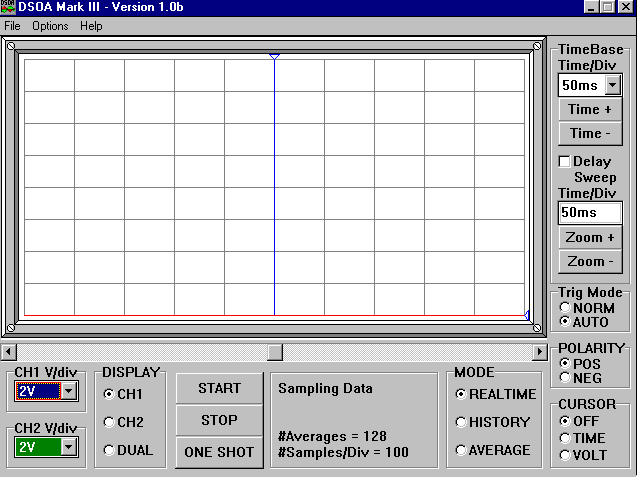
The Windows program has several features asked for from previous users of the
Mk1 and Mk2 software, including : Time and voltage cursors allowing direct
readout of the time or voltage parameter between the cursors. Averaging,
which can be set from 2 to 128 averages is useful for removing uncorrelated
noise from a waveform. A history function, which provides a "persistance"
type display that retains previous waveforms on screen. This is useful for
finding intermittent problems over an extended period of time. A second
timebase allows you to "zoom" in on a waveform and scroll from side to side.
Waveforms can be saved to disk in either binary or text format, useful for
importing the data into spreadsheets for later analysis. The program can also
do a direct screen printout to any Windows compatible printer. Requirements
for the Windows program are Windows 3.1 or later, at least 640x480 16-colour
VGA screen mode, and a mouse. The program only requires several hundred
kilobytes of memory.
That's all there is to the DSOA Mk3, I hope you find it a valuable addition
to your test gear.
WARNING :
The DSOA inputs are NOT floating, and are connected to mains earth via the
ground connection on the PC parallel port. Therefore, as with any CRO,
extreme care should be taken when using the DSOA on earthed equipment. Do NOT
connect the ground lead of the CRO probe to any voltage which is referenced
to mains earth. Doing so is extremely dangerous and will damage the DSOA
and/or your computer !.
SEMICONDUCTORS :
TDA8703 2
LM741 2
LM6361N 4
AD744 2
LM319 1
74HCT574 2
ULN2003A 1
74HC257 2
AM7202A-35RC (Skinny DIP) 2
74HC107 1
74HC86 1
74HC74 1
74HC20 1
74HC390 2
74HC151 1
20MHz XTAL OSC. MODULE 1
7805 REGULATOR (TO-220) 1
7812 REGULATOR (TO-220) 1
7912 REGULATOR (TO-220) 1
1N914 DIODE 6
1N4002 DIODE 2
5mm RED LED 1
8-PIN DUAL WIPE IC SOCKETS 8
14-PIN DUAL WIPE IC SOCKETS 10
16-PIN DUAL WIPE IC SOCKETS 6
20-PIN DUAL WIPE IC SOCKETS 2
24-PIN DUAL WIPE IC SOCKETS 2
CAPACITORS :
100nF 0.2 PITCH MONO 33
10uF 0.2 PITCH 16V TANTULUM 4
470uF 25V ELECTRO 1
2200uF 25V ELECTRO 1
5-30pF TRIMMER CAP 2
150pF 0.2 PITCH CERAMIC 2
5.6pF 0.1 PITCH CERAMIC 2
RESISTORS :
47R 1% 3
1K 1% 14
68R 1% 2
470R 1% 4
220R 1% 2
390R 1% 2
1K5 1% 2
2K2 1% 2
4K7 1% 2
6K8 1% 2
100K 1% 3
220K 1% 2
680K 1% 2
10K LINEAR POT 2
1K LINEAR POT 1
MISC :
SPDT CENTRE-OFF SWITCH 2
12V DPDT MINI DIL PCB RELAY
(MATSUSHITA TQ2 OR SIMILAR) 6
KNOBS 3
SMALL TO-220 HEATSINK 1
IEC FUSED PANEL MOUNT SOCKET 1
BNC PANEL SOCKET 2
D25 IDC SOCKET 1
26 WAY IDC HEADER SOCKET 1
26 WAY DUAL ROW HEADER PINS 1
12.6VAC 500mA TRANSFORMER 1
260(W)x180(D)x65(H) CASE
(WITH ALUMINIUM FRONT PANEL) 1
BLANK COPPER CLAD PCB
(100mm x 100mm) 1
PCB STANDOFFS 4
RG-174 COAXIAL CABLE 300mm
26 WAY RIBBON CABLE 150mm
TINNED COPPER WIRE
PCB (Code DSOA331) 1


|
|
|
| |
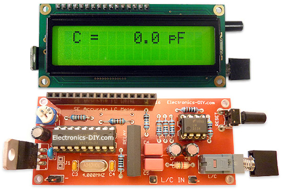
Accurate LC Meter
Build your own Accurate LC Meter (Capacitance Inductance Meter) and start making your own coils and inductors. This LC Meter allows to measure incredibly small inductances making it perfect tool for making all types of RF coils and inductors. LC Meter can measure inductances starting from 10nH - 1000nH, 1uH - 1000uH, 1mH - 100mH and capacitances from 0.1pF up to 900nF. The circuit includes an auto ranging as well as reset switch and produces very accurate and stable readings. |
|
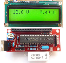
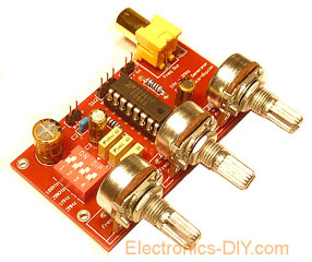
PIC Volt Ampere Meter
Volt Ampere Meter measures voltage of 0-70V or 0-500V with 100mV resolution and current consumption 0-10A or more with 10mA resolution. The meter is a perfect addition to any power supply, battery chargers and other electronic projects where voltage and current must be monitored. The meter uses PIC16F876A microcontroller with 16x2 backlighted LCD. |
|
|
|
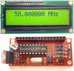
60MHz Frequency Meter / Counter
Frequency Meter / Counter measures frequency from 10Hz to 60MHz with 10Hz resolution. It is a very useful bench test equipment for testing and finding out the frequency of various devices with unknown frequency such as oscillators, radio receivers, transmitters, function generators, crystals, etc. |
|
1Hz - 2MHz XR2206 Function Generator
1Hz - 2MHz XR2206 Function Generator produces high quality sine, square and triangle waveforms of high-stability and accuracy. The output waveforms can be both amplitude and frequency modulated. Output of 1Hz - 2MHz XR2206 Function Generator can be connected directly to 60MHz Counter for setting precise frequency output. |
|
|
|
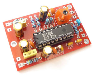
BA1404 HI-FI Stereo FM Transmitter
Be "On Air" with your own radio station! BA1404 HI-FI Stereo FM Transmitter broadcasts high quality stereo signal in 88MHz - 108MHz FM band. It can be connected to any type of stereo audio source such as iPod, Computer, Laptop, CD Player, Walkman, Television, Satellite Receiver, Tape Deck or other stereo system to transmit stereo sound with excellent clarity throughout your home, office, yard or camp ground. |
|
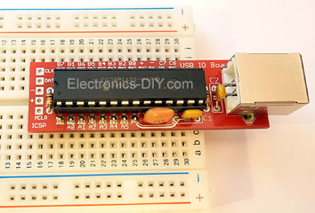
USB IO Board
USB IO Board is a tiny spectacular little development board / parallel port replacement featuring PIC18F2455/PIC18F2550 microcontroller. USB IO Board is compatible with Windows / Mac OSX / Linux computers. When attached to Windows IO board will show up as RS232 COM port. You can control 16 individual microcontroller I/O pins by sending simple serial commands. USB IO Board is self-powered by USB port and can provide up to 500mA for electronic projects. USB IO Board is breadboard compatible. |
|
|
|
|
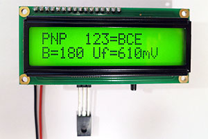
ESR Meter / Capacitance / Inductance / Transistor Tester Kit
ESR Meter kit is an amazing multimeter that measures ESR values, capacitance (100pF - 20,000uF), inductance, resistance (0.1 Ohm - 20 MOhm), tests many different types of transistors such as NPN, PNP, FETs, MOSFETs, Thyristors, SCRs, Triacs and many types of diodes. It also analyzes transistor's characteristics such as voltage and gain. It is an irreplaceable tool for troubleshooting and repairing electronic equipment by determining performance and health of electrolytic capacitors. Unlike other ESR Meters that only measure ESR value this one measures capacitor's ESR value as well as its capacitance all at the same time. |
|
Audiophile Headphone Amplifier Kit
Audiophile headphone amplifier kit includes high quality audio grade components such as Burr Brown OPA2134 opamp, ALPS volume control potentiometer, Ti TLE2426 rail splitter, Ultra-Low ESR 220uF/25V Panasonic FM filtering capacitors, High quality WIMA input and decoupling capacitors and Vishay Dale resistors. 8-DIP machined IC socket allows to swap OPA2134 with many other dual opamp chips such as OPA2132, OPA2227, OPA2228, dual OPA132, OPA627, etc. Headphone amplifier is small enough to fit in Altoids tin box, and thanks to low power consumption may be supplied from a single 9V battery. |
|
|
|
|
|
Arduino Prototype Kit
Arduino Prototype is a spectacular development board fully compatible with Arduino Pro. It's breadboard compatible so it can be plugged into a breadboard for quick prototyping, and it has VCC & GND power pins available on both sides of PCB. It's small, power efficient, yet customizable through onboard 2 x 7 perfboard that can be used for connecting various sensors and connectors. Arduino Prototype uses all standard through-hole components for easy construction, two of which are hidden underneath IC socket. Board features 28-PIN DIP IC socket, user replaceable ATmega328 microcontroller flashed with Arduino bootloader, 16MHz crystal resonator and a reset switch. It has 14 digital input/output pins (0-13) of which 6 can be used as PWM outputs and 6 analog inputs (A0-A5). Arduino sketches are uploaded through any USB-Serial adapter connected to 6-PIN ICSP female header. Board is supplied by 2-5V voltage and may be powered by a battery such as Lithium Ion cell, two AA cells, external power supply or USB power adapter. |
|
200m 4-Channel 433MHz Wireless RF Remote Control
Having the ability to control various appliances inside or outside of your house wirelessly is a huge convenience, and can make your life much easier and fun. RF remote control provides long range of up to 200m / 650ft and can find many uses for controlling different devices, and it works even through the walls. You can control lights, fans, AC system, computer, printer, amplifier, robots, garage door, security systems, motor-driven curtains, motorized window blinds, door locks, sprinklers, motorized projection screens and anything else you can think of. |
|
|
|